European Technology Symposium 2024: TSMC Ready to Manufacture Next-Gen HBM4 Base Dies
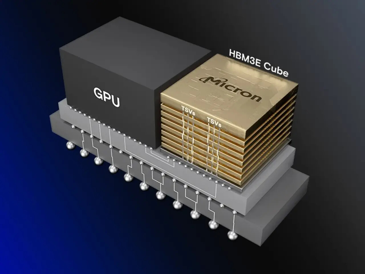
At the European Technology Symposium 2024, TSMC has announced its preparedness to produce next-generation HBM4 base dies using both 12 nm and 5 nm nodes. This significant advancement is anticipated to greatly enhance the performance, power efficiency, and logic density of HBM4 memory, meeting the requirements of high-performance computing (HPC) and artificial intelligence (AI) applications. The transition from a traditional 1024-bit interface to an ultra-wide 2048-bit interface is a crucial aspect of the new HBM4 standard. This modification will allow for the incorporation of more logic and improved performance while reducing power consumption. TSMC will utilize its N12FFC+ and N5 processes to manufacture these base dies, with the N12FFC+ process offering a cost-effective solution for achieving HBM4 performance and the N5 process delivering even more logic and lower power consumption at HBM4 speeds.
The company is working in collaboration with major HBM memory partners such as Micron, Samsung, and SK Hynix to integrate advanced nodes for full-stack integration of HBM4. TSMC's base die, produced using the N12FFC+ process, will be utilized to mount HBM4 memory stacks on a silicon interposer alongside system-on-chips (SoCs). This configuration will enable the development of 12-Hi (48 GB) and 16-Hi (64 GB) stacks with per-stack bandwidth exceeding 2 TB/s. TSMC's partnership with EDA partners like Cadence, Synopsys, and Ansys ensures the reliability of HBM4 channel signals, thermal accuracy, and electromagnetic interference (EMI) in the new HBM4 base dies. TSMC is also optimizing CoWoS-L and CoWoS-R for HBM4 integration, indicating that large high-performance chips are already leveraging this technology and gearing up for mass production.