Intel Demonstrates Latest Transistor Advancements at IEEE IEDM
During the 69th annual IEEE International Electron Devices Meeting (IEDM), Intel showcased its latest developments in transistor design and manufacturing. One notable advancement is the 3D integration of transistors. Intel has successfully stacked complementary field effect transistors (CFET) with a scaled gate pitch as small as 60 nm. This 3D stacked CFET technology allows for higher density by utilizing both vertical and horizontal space. Intel's 7 node already has a 54 nm gate pitch, bringing CFETs close to matching production-ready nodes. With further refinement, we can expect to see 3D stacked CFETs in production runs in the near future.
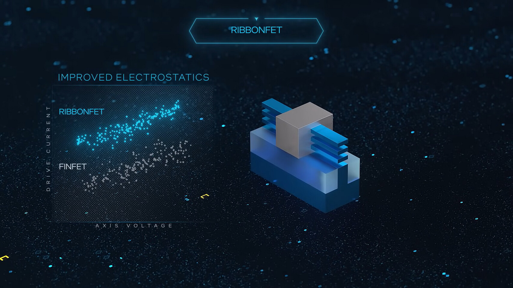
Another breakthrough is Intel's RibbonFET technology, which introduces a new transistor architecture. Unlike the FinFET introduced in 2012, RibbonFET uses ribbon-shaped channels surrounded by the gate. This design enables better control and higher drive current at all voltage levels, resulting in faster transistor switching speeds and improved frequency and performance. The width of the nanoribbon channels can be adjusted based on the application's requirements, allowing for thinner channels in low-power mobile applications and wider channels in high-performance applications. Despite its smaller footprint, a single stack of nanoribbons can achieve the same drive current as multiple fins in FinFET.
Intel also announced that its PowerVia technology is ready for production, with the first products utilizing PowerVia expected to launch in 2024. PowerVia aims to optimize transistor power delivery by relocating the power routing wires from the top to below the transistor. This improves power management and prevents interference with signal wires on the top of the transistor. PowerVia utilizes nano through silicon vias (TSVs), which are 500 times smaller than regular TSVs, to connect to the transistor layer.
In addition, Intel demonstrated the successful integration of silicon and GaN, resulting in a high-performance integrated circuit solution called "DrGaN" for power delivery. This solution has the potential to meet the power density and efficiency demands of future computing. Intel will also present transition metal dichalcogenide (TMD) 2D channel materials, which offer a scaling path for transistor physical gate length below 10 nm. Prototypes of high-mobility TMD transistors for NMOS and PMOS elements will be showcased. Lastly, Intel will present the world's first gate-all-around (GAA) 2D TMD PMOS transistor and the world's first 2D PMOS transistor fabricated on a 300 mm wafer, both aimed at further scaling transistor density.